PRESENTS:
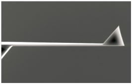
The most often used standard probe for ultra-high speed scanning is the NanoWorld A R R O W ™ UHF
The Arrow™ UHF (Ultra High Frequency) is a silicon SPM and AFM probe with a tetrahedral tip and a triangular cantilever capable of resonating with an ultra high frequency of up to
2.0 MHz. On request, specific cantilever thicknesses are selected within very narrow tolerances for
an extra selection fee.
The Arrow UHF is optionally also available wth a gold reflex coating.
For more developments for the emerging field of
high speed scanning please have a look below.
Cantilever 3D View
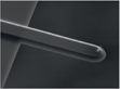
Cantilever Top View
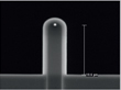
Tip Front View
Tip Detail
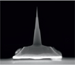
Support Chip 3D View
U l t r a - S h o r t - A F M - C a n t i l e v e r s
Next generation of AFM Probes for High Speed Scanning
Concept
- development of very short, narrow and thin cantilevers with Electron Beam Deposited
(EBD) tip for High Speed Scanning applications for present and future AFM systems - different cantilever materials are evaluated:
Si (poly/single crystal/111), SiN, New Material ("NM") - joint development between NanoWorld AG and nanotools GmbH
Description of Ultra-Short-AFM-Cantilevers (USC) made of New Material
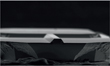
Cantilevers
- different prototypes of Ultra-Short cantilevers have been developed and
fabricated resulting in different mechanical properties:
calculated values
| Resonance Frequency [kHz] | 5000 | 2000 | 1500 | 330 | 1300 | 1250 | 500 |
| Force Constant [N/m] | 30 | 3.0 | 0.6 | 0.3 | 1.2 | 7.8 | 0.75 |
| CB length [m] | 10 | 10 | 7 | 20 | 10 | 20 | 20 |
| CB width [m] | 5 | 5 | 3 | 10 | 5 | 10 | 10 |
| CB thickness [nm] | 680 | 280 | 100 | 190 | 190 | 680 | 280 |
Tip
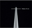
- nanotools® High Dense Carbon (HDC) tip with the following dimensions:
Height: > 2.0 m (typically 2.5
m)
Tip radius: < 10 nm
Aspect ratio: approx. 1:5
Tilt compensation: 8±1 deg
Support chip
- dimensions of the Si support chip are very reproducible (1.6 mm x 3.4 mm)
- etched and lowered corners of the Si support chip avoid contact
between the Si support chip and the sample
Coating
- 30 nm Gold reflex coating on both sides of the cantilevers (tip uncoated)
Status
- prototypes available (have been validated by external tests)
- pre-production status: more than 50 wafers have been fabricated
- ongoing beta testing
More information on www.highspeedscanning.com
For more information you can visit www.nanoandmore.com
Comments