PRESENTS:

AFM Measurements on GaN Quantum Dots - Comparison
of different commercially available Probe Types
Corresponding Authors: O. Krause, krause@nanosensors.com C. Richter, richter@nanosensors.com
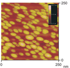
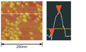
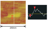
FIG. 1: AFM Image of GaN Quantum Dots on AIN
Topography measured with a SuperSharpSilicon™Tip
We perfomed high resolution AFM measurements on GaN Quantum Dots
(QDs) with different AFM probes (FIG. 3 to Fig.S).
Because of their well defined dimensions (lateral as well as vertical) in the
nanometer scale and their high density on substrate QDs (FIG. 2) are an
ideal structure to benchmark AFM probes concerning their resolution at
small structures.
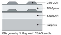 FIG. 2: Schematic Structure of GaN Quantum Dots on AIN
High Perfomance
AFM-Probe
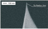
FIG. 3: SEM Picture of a SuperSharpSilicon™ Tip
Due to the tip radius of better than 5nm and
the excellent aspect ratio at the very end of
the tip every QD can be displayed exactly.
Standard Silicon
AFM-Probe
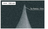
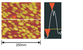
FIG. 4: SEM Picture of a Pointprobe Probe
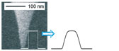
Single QDs can be imaged well using this
probe type (radius<15nm), but at high density areas Qds cannot be separated very sharply.
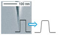
Silicon Nitride
AFM-Probe
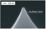
FIG. 5: SEM Picture of a typical Silicon Nitride AFM-Probe

The reduced tip radius of about 25nm and
the worse aspect ratio at the end of the tip
do not allow a "true visualisation" of QDs.

For more information you can visit www.nanoandmore.com
Comments