PRESENTS:

Platinum silicide probes: highly conductive AFM probes with small radii and high wear resistance
Conductive diamond
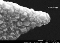
Conductive diamond probes. Advantages: hard, long-lasting coating. Disadvantages: large radius, low conductivity
The best of both worlds
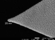
Platinum silicide probes
Advantages: small radius, excellent conductivity, good wear-out behavior
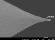
Platinum coated probes
Platinum(Iridium) coated probes. Advantages: relatively small radius, excellent conductivity. Disadvantages: fast wear-out
Extremely durable: C-AFM comparison of PtSi and Pt probes
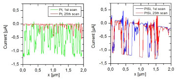
Cross sections of current images of (a) a commercial Pt probe (Pt, left image) and (b) a PtSi probe (PtSi, right image).
TUNA mode, DI Icon, sample bias -0.25V, force 1μN, total tip travel distance 13mm. For each tip a cross section out of the first
and the last scan is shown.
Silicide tip advantages
- Formation of a hard and massive conductive tip apex instead of only a few ten nanometer deposited metal coating at the tip apex
- Smaller radius than PtIr coated probes. About 5 to 6 times smaller than diamond coated tips
- Metal (PtIr) like conductivity. About 10 times better conductivity than conductive diamond
- Dramatically reduced wear rates compared to silicon and PtIr coated tips
Product list
| Type | Application | Force Constant [N/m] (nominal) |
Res. Frequency [kHz] (nominal) |
Coating (backside) | |
| Non-Contact | PtSi-NCH | C-AFM, TUNA | 42 | 330 | PtSi (PtSi reflective) |
| PtSi-FM | C-AFM, TUNA, SCM EFM, KPFM, |
2.8 | 75 | PtSi (PtSi reflective) |
|
| Contact | PtSi-CONT 0.2 | C-AFM, TUNA, SCM |
0.2 | 13 | PtSi (PtSi reflective) |
| AVAILABLE SOON | |||||

For more information you can visit www.nanoandmore.com
Comments